Purpose
The RT5796A is a high efficiency synchronous step-down DC/DC converter. Its input voltage range is from 2.5V to 6V and provides an adjustable regulated output voltage from 0.6V to 3.4V while delivering up to 1.5A of output current.This document explains the function and use of the RT5796A evaluation board (EVB), and provides information to enable operation, modification of the evaluation board and circuit to suit individual requirements.
Introduction
General Product Information
The RT5796A is a high efficiency synchronous step-down DC/DC converter. Its input voltage range is from 2.5V to 6V and provides an adjustable regulated output voltage from 0.6V to 3.4V while delivering up to 1.5A of output current. The internal synchronous low on-resistance power switches increase efficiency and eliminate the need for an external Schottky diode. The Current Mode Constant-On-time (CMCOT) operation with internal compensation allows the transient response to be optimized over a wide range of loads and output capacitors. The RT5796A is available in the TSOT-23-6 package.
Product Feature
-
Efficiency Up to 95%
-
RDSON 160mΩ HS/110mΩ LS
-
VIN Range 2.5V to 6V
-
VREF 0.6V with ±2% Accuracy
-
CMCOT™ Control Loop Design for Best Transient Response, Robust Loop Stability with Low-ESR (MLCC) COUT
-
Fixed Soft-Start 1.2ms; PGOOD Function in TSOT-23-6
-
Cycle-by-Cycle Over Current Protection
-
Input Under Voltage Lockout
-
Output Under Voltage Protection (UVP Hiccup)
-
Thermal Shutdown Protection
-
Power Saving at Light Load
Key Performance Summary Table
|
Key Features
|
Evaluation Board Number : PCB070_V1
|
|
Default Input Voltage
|
3.3V
|
|
Max Output Current
|
1.5A
|
|
Default Output Voltage
|
1.2V
|
|
Default Marking & Package Type
|
RT5796AHGJ6, TSOT-23-6
|
|
Operation Frequency
|
Steady 1MHz at all loads
|
Bench Test Setup Conditions
Headers Description and Placement
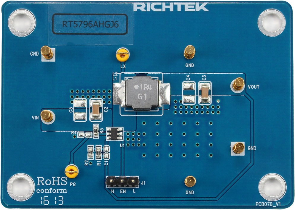
Please carefully inspect the EVB IC and external components, comparing them to the following Bill of Materials, to ensure that all components are installed and undamaged. If any components are missing or damaged during transportation, please contact the distributor or send e-mail to evb_service@richtek.com.
Test Points
The EVB is provided with the test points and pin names listed in the table below.
|
Test point/
Pin name
|
Signal
|
Comment (expected waveforms or voltage levels on test points)
|
|
FB
|
Feedback Voltage Input
|
Feedback Voltage Input. An external resistor divider from the output to GND, tapped to the FB pin, sets the output voltage.
|
|
VIN
|
Input voltage
|
Supply Voltage Input. The RT5796A operates from a 2.5V to 6V unregulated input. C1 is needed to prevent large voltage spikes from appearing at the input.
Quiet ground for controller circuits.
|
|
GND
|
Ground
|
Power Ground and Quiet Ground for Controller Circuits.
|
|
PG
|
Power Good Indicator
|
Power Good Indicator. The output of this pin is an open-drain with external pull-up resistor to IN. PG is pulled up to IN when the FB voltage is within 90%, otherwise it is LOW.
|
|
LX
|
Switch node
|
Switch node.
|
|
EN
|
Enable Control Input
|
Enable Control Input.
|
Power-up & Measurement Procedure
1. Apply a 3.3V nominal input power supply (2.5V < VIN < 6V) to the VIN and GND terminals.
2. Set the jumper at JP1 to connect terminals 2 and 3, connecting EN to VIN.
3. Verify the output voltage (approximately 1.2V) between VOUT and GND.
4. Connect an external load up to 1.5A to the VOUT and GND terminals and verify the output voltage and current.
Output Voltage Setting
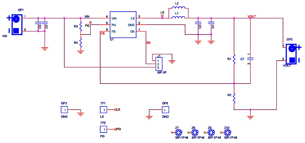
Set the output voltage with the resistive divider (R1, R2) between VOUT and GND with the midpoint connected to FB. The output is set by the following formula :
VOUT = VREF x (1 + R1 / R2)
Schematic, Bill of Materials & Board Layout
EVB Schematic Diagram
Bill of Materials
|
Reference
|
Qty
|
Part Number
|
Description
|
Package
|
Manufacture
|
|
U1
|
1
|
RT5796AHGJ6
|
DC/DC Converter
|
TSOT-23-6
|
RICHTEK
|
|
C1
|
1
|
|
NC
|
C-0603
|
|
|
C2, C3
|
2
|
C3216X5R1H106KT000N
|
10µF/50V/X5R/1206
|
C-1206
|
TDK
|
|
C4, C5
|
2
|
|
NA
|
C-1210
|
|
|
L1
|
1
|
NR8040T1R4N
|
1.4µH
|
L-NR8040_2
|
TAIYO YUDEN
|
|
R1, R2, R3
|
3
|
0603 100K 1%
|
100k
|
R-0603
|
WALSIN
|
|
R4
|
1
|
|
NC
|
R-0603
|
|
PCB Layout
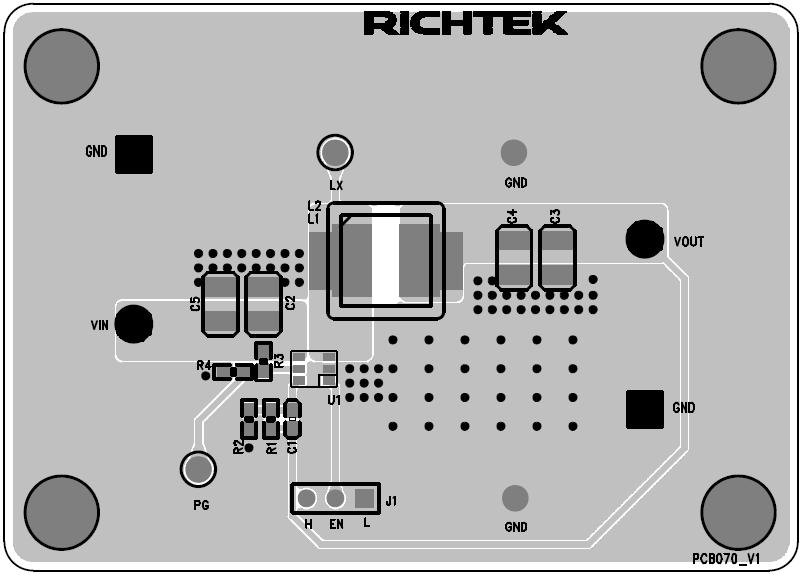
Top View
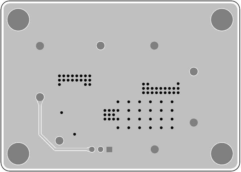
Bottom View